Microprocessors Final Project: PicoWord 32
Introduction
This is a writeup on my final project for the Microprocessors I course at UMass Lowell (ECE department).
PicoWord 32 is a 32-bit binary-to-decimal converter. It reads a 32-bit binary value entered via 32 DIP switches using four daisy-chained SN74HC165 Parallel-In Serial-Out (PISO) shift registers, converts the 32-bit value into a 10-digit decimal number, and outputs the result in real time across ten 7-segment LED displays driven by ten daisy-chained SN74LS164 Serial-In Parallel-Out (SIPO) shift registers.
While the project was originally intended to be written entirely in ARMv6-M Thumb assembly for the Raspberry Pi Pico (RP2040), the final functional hardware implementation was completed in C++ using the Arduino framework.
The complete firmware repository is available on Github: PicoWordC-32 Code Base
Specifications
| Parameter | Specification |
|---|---|
| Microcontroller | Raspberry Pi Pico (RP2040 Dual ARM Cortex-M0+) |
| Input Capacity | 32-bit Binary (0 to 4,294,967,295) via 32 DIP switches |
| Input Shift Registers | 4× SN74HC165 (8-bit PISO, daisy-chained) |
| Output Displays | 10× Common Anode/Cathode 7-Segment LED Displays |
| Output Shift Registers | 10× SN74LS164 (8-bit SIPO, daisy-chained) |
| Logic Level Conversion | 2N3904 NPN Inverter Level-Shifter Array (3.3V TTL → 5V TTL) |
| Target Clock Frequency | ~100 kHz |
| Implementation Language | C++ (Arduino Framework) |
System Architecture
The overall hardware and logic architecture consists of three core stages:
- Parallel Binary Input Stage (PISO): Read 32 individual DIP switches into a 4-byte serial register chain.
- RP2040 Processing & Translation: Capture binary input, store as a 32-bit unsigned integer (
uint32_t), extract individual decimal digits (0–9), and encode each digit into 7-segment bitmasks. - Serial Display Output Stage (SIPO): Clock the encoded 10-byte segment array serially through ten daisy-chained shift registers to update the 7-segment displays.

Hardware Block Diagram

For higher resolution schematic documents, refer to the PDF files below:
Hardware Implementation
1. Input Stage: SN74HC165 PISO Shift Registers
The 32-bit input uses four 8-bit SN74HC165 PISO shift registers daisy-chained together.
- Each DIP switch connects to a parallel input pin on the SN74HC165.
- The RP2040 controls the register chain using three control lines:
- SH/LD (Shift/Load): Pulls low to latch the physical 32-bit DIP switch state into the register array, then returns high to enable serial shifting.
- CLK (Clock): Clocks serial bits out of the register chain.
- DATA_IN (Serial Data Input): Reads bit states into the RP2040 GPIO pins.

Note: Proper resistor configurations (pull-down/pull-up) are required on the DIP switch pins to prevent floating inputs. Early wiring required careful debugging to ensure switch position logic matched input expectations.

2. Level Shifting & Logic Level Conversion (3.3V to 5V TTL)
The Raspberry Pi Pico operates on 3.3V logic, whereas the 74HC and 74LS series ICs on the breadboard operate reliably at 5V TTL levels. Additionally, long breadboard power rails and parasitic wire capacitance can cause 3.3V signals to degrade quickly.
To solve this, custom transistor-based NOT gates (inverters) were constructed for each RP2040 output signal to convert 3.3V TTL to 5V TTL:
- Transistor: 2N3904 NPN BJT
- Base Input Resistor: 10kΩ (limits current drawn from RP2040 GPIO pins)
- Collector Pull-up Resistor: 1kΩ tied to +5V VCC
When the Pico GPIO outputs HIGH (3.3V), the 2N3904 turns ON, pulling the collector LOW (0V). When GPIO outputs LOW (0V), the transistor turns OFF, allowing the 1kΩ pull-up resistor to pull the line cleanly up to 5V. Inverting the signal twice (or accounting for logic inversion in firmware) provides robust 5V logic drive.
3. Output Stage: SN74LS164 SIPO Shift Registers
To drive ten 7-segment displays without needing 70+ GPIO pins, ten SN74LS164 8-bit SIPO shift registers are cascaded end-to-end.
- The serial output pin (QH) of each SN74LS164 is connected to the serial input pin (A/B) of the next register in the chain.
- A single shared clock line toggles all ten registers simultaneously.
- 10 bytes (80 total bits) are shifted serially through the line:
- 7 bits control segments A through G.
- 1 bit controls the Decimal Point (DP).

7-Segment Encoding Reference
| Digit | Active Segments | Coded Bitmask (MSB...LSB: DP, G, F, E, D, C, B, A) |
|---|---|---|
| 0 | A, B, C, D, E, F | 0b00111111 |
| 1 | B, C | 0b00000110 |
| 2 | A, B, D, E, G | 0b01011011 |
| 3 | A, B, C, D, G | 0b01001111 |
| 4 | B, C, F, G | 0b01100110 |
| 5 | A, C, D, F, G | 0b01101101 |
| 6 | A, C, D, E, F, G | 0b01111101 |
| 7 | A, B, C | 0b00000111 |
| 8 | A, B, C, D, E, F, G | 0b01111111 |
| 9 | A, B, C, F, G | 0b01100111 |
Software & Firmware Pipeline
The RP2040 firmware operates in an active processing loop using GPIO interrupts and timers:
// High-level conceptual representation of the PicoWord firmware loop
uint32_t raw_binary_input = read_piso_shift_registers(); // Reads 32 bits serially

// Convert 32-bit unsigned integer to decimal digit array
uint8_t decimal_digits[10];
for (int i = 9; i >= 0; i--) {
    decimal_digits[i] = raw_binary_input % 10;
    raw_binary_input /= 10;
}

// Map each decimal digit to its corresponding 7-segment bitmask
uint8_t segment_output_bytes[10];
for (int i = 0; i < 10; i++) {
    segment_output_bytes[i] = segment_lookup_table[decimal_digits[i]];
}

// Shift out 10 bytes serially to the ten 74LS164 SIPO shift registers
write_sipo_shift_registers(segment_output_bytes, 10);
By leveraging hardware GPIO interrupts for serial clocking, the firmware ensures zero missed switch transitions and achieves seamless real-time response as DIP switches are toggled.
Signal Integrity & Oscilloscope Debugging
During initial hardware testing on breadboards, severe bit-flip errors, corruption, and unstable digit output occurred when updating the display chain at the target 100 kHz clock speed.
Using an Analog Discovery Kit oscilloscope, signal traces revealed that the root cause was the transistor level-shifter pull-up resistance.
The 10kΩ Pull-Up Issue
Originally, 10kΩ resistors were used as collector pull-ups on the 2N3904 NPN transistors. At 100 kHz, the RC time constant formed by the 10kΩ resistance and parasitic capacitance across the long breadboard rails degraded the pulse waveforms.

As shown in the waveform above, Channel 2 (blue) exhibits a slow exponential RC charging curve. The signal barely reaches ~2.2V before the line is pulled back down, missing the valid TTL HIGH threshold and causing bit drops across the shift registers.
The 1kΩ Pull-Up Solution
Replacing the 10kΩ collector pull-up resistors with 1kΩ resistors increased drive current and drastically reduced the RC time constant.

With 1kΩ resistors installed, Channel 2 (blue) shows a rapid voltage rise with crisp square edges up to 5V TTL levels. This eliminated all bit corruption and timing errors across all 14 shift registers.
Final Assembly & Testing
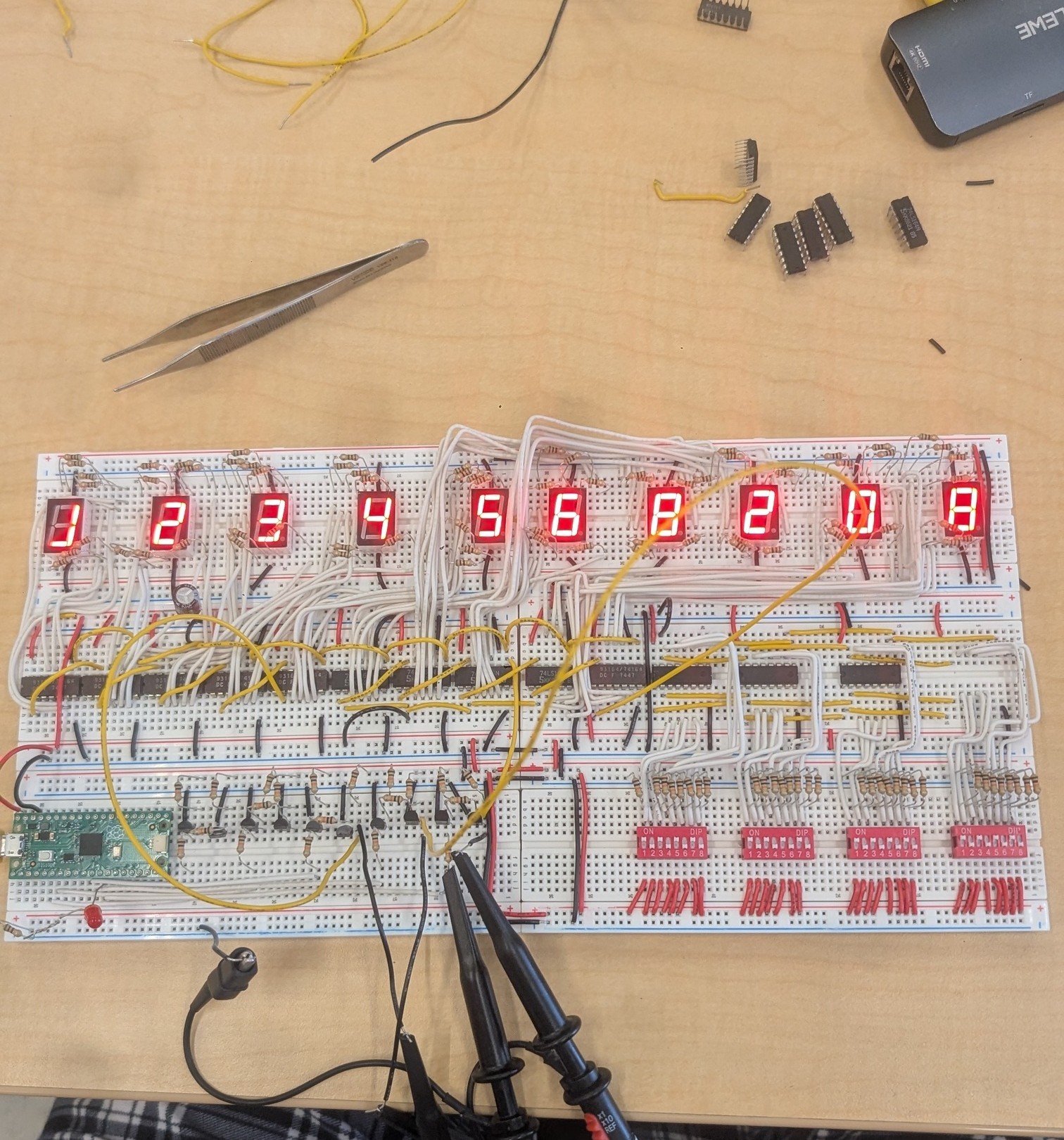
Completed Breadboard System
Below is the fully populated, operational breadboard setup with all 32 switches, level shifters, 14 shift registers, and 10 displays displaying numbers 0 1 2 3 4 5 6 7 8 9:


Functional Testing Videos
Real-Time Switch Input Testing
Full Output Display Testing
High-Speed Refresh Testing
Debugging Shift Input Hardware
Conclusion & Lessons Learned
The PicoWord 32 project successfully met the majority of core goals for the UMass Lowell Microprocessors I final project (excluding the final codebase being entirely written in ARMv6 Assembly):
- 32-bit Binary Input to Decimal Output: Correctly converts large 32-bit values up to 4,294,967,295 into decimal digits displayed across ten 7-segment displays.
- Cascaded Shift Register Architecture: Successfully operated 14 cascaded shift registers (4 PISO, 10 SIPO) synchronously from a single RP2040.
- Hardware Signal Debugging: Diagnosed and resolved 3.3V vs 5V logic degradation and RC delay issues using oscilloscope waveform analysis.
Future Improvements
If iterating on this design in the future:
- Dedicated PCB Design: Replacing the vast breadboard jumper wire loom with a custom multi-layer PCB to eliminate parasitic capacitance and reduce footprint.
- Dedicated Level-Shifter ICs: Using integrated 74HCT series buffers or TXS0108E logic level translators instead of discrete NPN transistor inverters.
- Pure Assembly Port: Completing the bare-metal ARMv6-M Thumb assembly version to satisfy the initial theoretical challenge without SDK dependencies.